
Insights
- At advanced nodes, growing chip complexity and tighter PPA demands are pushing manual physical design beyond its limits.
- Traditional physical design optimizes each stage in isolation, creating compounding inefficiencies, frequent rework, and unpredictable design cycles.
- Generative AI reasons across the entire physical design lifecycle, combining structural awareness with adaptive decision-making to continuously improve design quality.
- AI-driven physical design compresses multi-week floorplan and placement cycles into hours, enabling faster product launches and more predictable time-to-market.
- Realizing sustained value requires embedding generative AI into the fabric of design workflows — across data, toolchains, engineering roles, and governance — not treating it as a pilot or add-on.
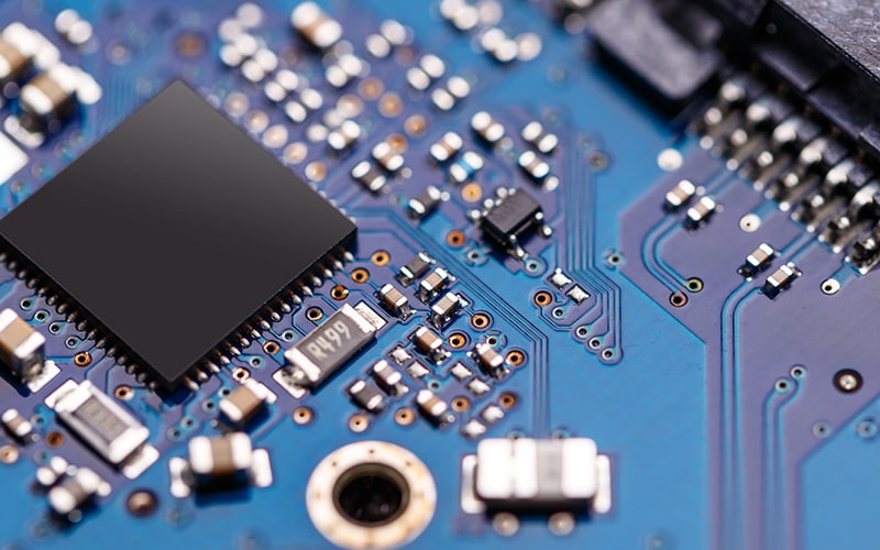
As semiconductors power everything from artificial intelligence (AI) to 5G and automotive systems, the physical design of semiconductor chips has become one of the most challenging and consequential stages of the development life cycle. At advanced nodes, typically referring to manufacturing technologies at 5 nanometers and below, chips pack far more transistors and connections into the same area, making them harder to organize, connect, and power efficiently. This growing complexity affects all stages of the physical design process, including floorplanning, placement, clock tree synthesis (CTS), and routing. Achieving optimal power, performance, and area (PPA) requires careful coordination across these interdependent steps, often under aggressive time-to-market constraints.
Why is physical design harder to scale?
Each stage of physical design plays a critical role in shaping final silicon outcomes. At advanced nodes, however, the increased density results in higher complexity, tighter interdependencies, and reduced margin for error.
Despite this shift, physical design is still executed as a largely manual and expert driven process, optimized one stage at a time. As design complexity grows, this approach becomes harder to scale, leading to prolonged and unpredictable design cycles, frequent rework, and outcomes that fall short of targeted PPA goals.
Stage 1: Floorplanning
Floorplanning defines the chip’s physical layout by deciding where major building blocks such as processors, memory, and other specialized components are placed and how they are connected to each other. These early choices strongly influence the chip’s size and shape, wiring and power delivery, shaping later design stages. However, floorplanning often consumes a high share of the overall design timeline between 15% and 20%. Because these decisions are made with limited downstream visibility, early congestion or power grid issues frequently resurface later, increasing late stage design risk.
Stage 2: Placement
Placement determines the exact locations of the chip’s smallest logic elements, arranging millions or even billions of cells within the floorplan. While floorplanning sets the overall structure, placement determines how smoothly signals move between nearby blocks and whether wiring can be completed without excessive crowding. Small inefficiencies introduced here can have an outsized impact later. For instance, a 10% wirelength increase can require 15% more power. Local density and congestion can make later wiring far more difficult. As a result, placement often becomes a cycle of trial, adjustment, and readjustment rather than a clean progression forward.
Stage 3: CTS
CTS builds the network that distributes signals, known as the clock, to all parts of the chip, ensuring these signals arrive at different parts of the chip at nearly the same time, so operations stay synchronized. To compensate for any lags, CTS introduces buffers and carefully balances clock paths, a process that further adds power consumption and increases local wiring complexity. At advanced nodes, clock networks already consume a significant share of total chip power, making CTS a critical driver of both performance and energy efficiency. Small disruptions such as voltage drops or local congestion can distort clock behavior and increase the risk of late discovery issues forcing costly redesign cycles that can reach $25 million per re-spin.
Stage 4: Routing
Routing lays down the physical wiring that connects all parts of the chip. At advanced nodes, thinner and more densely packed wires increase resistance-capacitance (RC) delays, slowing signals and increasing energy consumption. Signal interference becomes harder to control, and unresolved constraints from earlier stages sharply limit flexibility. As a result, routing frequently becomes the final and most painful barrier to completing a design.
Taken together, these stages determine the achievable PPA, yield, and scalability. Each stage is fundamentally a geometry problem, and any weakness introduced early magnifies downstream. A poor decision at any point forces detour routes, increases delays and triggers engineering change order (ECO) iterations (Figure 1).
Figure 1. Physical design workflow

Source: Infosys
The generative AI shift
As physical design complexity continues to escalate at advanced nodes, incremental improvements are not sufficient. The growing number of constraints, interactions, and design permutations calls for an approach that can reason across the entire physical design life cycle, rather than optimizing each stage in isolation.
Generative AI introduces this shift. Rather than relying on static rules, it learns from historical layouts, design constraints, and performance outcomes to continuously generate and assess design alternatives. By refining decisions through feedback, generative AI can explore a much broader set of possibilities and reduce weeks of iteration to hours — accelerating physical design closure, reducing design cost, and increasing the likelihood of first-time-right silicon.
Generative AI can be applied to the physical design process by combining two complementary capabilities: graph neural network (GNN) and reinforcement learning (RL). Together, these capabilities enable AI systems to reason for physical design as a connected, evolving problem rather than as a sequence of isolated steps. These capabilities work independently, yet the combination of these techniques is particularly well suited to addressing the challenges of advanced-node physical design.
What is a GNN?
A GNN is a type of AI designed to work with graphs. A graph is a mathematical representation of objects, also called nodes, and their relationships, referred to as edges. In the context of chip design:
- Nodes represent functional blocks on the chip such as central processing unit, graphics processing unit (GPU) and memory.
- Edges represent connections and wires that carry signals between blocks such as the data bus connections and clock distribution.
Put simply, GNNs are designed to learn patterns and make predictions based on the structure of a graph.
What is RL?
RL learns by making decisions and improving them through experience. Instead of following predefined rules, an RL system explores different actions and learns which choices lead to better outcomes based on feedback. Applied to physical design, RL treats tasks such as block placement and optimization as a sequence of decisions, where each placement choice influences future options and overall design quality. Over multiple iterations, the RL agent learns strategies that maximize long term rewards. This leads to better placement decisions, faster convergence, and improved design outcomes.
GNN and RL: A powerful combination for physical design
When combined, GNNs provide structural awareness, while RL provides decision-making capability, enabling informed decisions throughout the physical design flow:
- During floorplanning, RL uses GNN insights to explore optimal macro- and block-level arrangements that minimize congestion and improve power delivery.
- In placement, it learns cell positioning strategies that balance timing, power, and congestion.
- During clock tree synthesis, the model helps ensure clock signals are distributed more evenly across the chip, reducing latency and improving overall timing consistency.
- Finally, for routing, the combined model iteratively refines choices to improve routability and meet closure goals.
Through continuous learning and multiple iterations, the generative AI system improves its ability to produce high quality layout options, driving faster convergence, better PPA tradeoffs, and more predictable physical design outcomes across the entire flow.
Key benefits of a generative AI approach
The generative AI approach delivers benefits across four dimensions — speed to market, silicon quality, engineering efficiency, and scalability — addressing both immediate design challenges and long term portfolio needs.
Speed to market
Compresses design-to-market timelines: Floorplan development cycles that traditionally take around 12 weeks, or nearly 480 hours, are consistently completed in under 36 hours, enabling up to 13 times faster product launches and measurable acceleration in time-to-revenue.
Silicon quality
Enhances PPA performance: An AI-driven approach delivers sustained PPA improvements across production designs. Learned layout optimizations shorten wirelength between three to five percent, reducing delays and congestion by about 30%, while improving overall energy efficiency. These gains enable about 9% faster timing closure and higher throughput, strengthening both design quality and competitive positioning.
Reduces clock and timing skew through learned topologies: By learning structural patterns from proven designs, GNN-based models identify timing-sensitive regions of the chip and guide placement toward more balanced clock paths. This includes assigning stronger or shorter connections where timing sensitivity is highest, resulting in an improvement of between 10% and 20% in clock arrival consistency across the chip early in the design flow. In addition, learned representations help flag regions prone to voltage drop that can affect signal timing, enabling earlier detection of critical areas and reducing late stage rework and redesign effort.
Engineering efficiency
Expands engineering throughput, without headcount increase: The AI-driven approach enables up to 60% faster layout completion, allowing teams to run more design iterations within the same project schedules. By increasing productivity with existing engineering teams, without adding headcount, it supports broader exploration of performance tradeoffs while maintaining delivery timelines.
Optimizes operational costs: By significantly reducing design reruns and manual rework, the AI driven approach lowers both labor and computing expenses across the physical design flow. Fewer late‑stage corrections reduce the number of long, resource-intensive design runs — lowering the overall demand on servers, computing time and cost, and infrastructure needed to complete the design. At the same time, it lets engineering teams focus more on innovation.
Scalability
Scales optimization across portfolios: By reusing learned placement strategies, AI-driven approach adapts quickly to new architectures and design variants, significantly shortening ramp-up for subsequent product lines. This reuse ensures consistent optimization quality, delivering uniform PPA improvements across products while reducing variability between designs.
Creates the foundation for agentic, self-optimizing physical design: A GNN-enhanced RL solution establishes a robust generative AI foundation, enabling optimized layouts, faster cycles, and adaptable design strategies. Over time, this framework can evolve into a modular agentic architecture, where autonomous agents collaborate across placement, rule validation, and layout refinement to enable scalable, continuous design improvement.
How to make generative AI a foundational capability
Adopting generative AI for semiconductor physical design requires deliberate investment across technology, people, and operating models. To realize sustained value and scale impact across design portfolios, semiconductor companies should focus on five strategic pillars.

Build a strong foundation for data readiness
Invest in building a unified physical design data lake that consolidates historical floorplans, placement iterations, ECO cycles, timing reports, and signoff outcomes. Normalize data ontologies across tools and projects to ensure consistency and reusability. Capture all intermediate decisions and corrective actions to allow AI models to learn how experts navigate tradeoffs, making future recommendations more robust and context aware.
Prepare the workforce for AI‑augmented design workflows
Rethink engineering roles. Train physical design teams on AI‑assisted workflows, enabling engineers to interpret model recommendations, guide optimization objectives, and validate outcomes. Create hybrid roles that combine physical design expertise with AI fluency and organize teams into physical design and AI pods to embed AI capabilities directly into day‑to‑day design execution.
Integrate AI directly into physical design processes and tools
Embed generative AI directly into the physical design flow rather than layering it on top as an add-on. Inject AI copilots into physical design stages, allowing AI insights to inform decisions early and continuously.
Invest in the right physical and compute infrastructure
Upgrade GPU infrastructure and establish secure, AI enabled physical design labs capable of handling sensitive design data. Establish dedicated physical design data centers with strong access controls to ensure proprietary IP remains protected while enabling rapid experimentation, model retraining, and iterative optimization across multiple design programs.
Establish governance, validation, and risk controls
Set up AI validation boards to define acceptable usage boundaries, validate model outputs, and manage risk. Establish robust controls around IP protection, access management, and hallucination mitigation to maintain trust in AI assisted workflows. Define clear accountability frameworks to ensure that AI recommendations are traceable, explainable, and aligned with silicon reliability and regulatory requirements.
As the appetite for smarter, faster, more power-efficient chips grows, semiconductor teams are being asked to deliver more complex designs more quickly, with less margin for rework cycles. Generative AI makes that expectation achievable by rethinking how chips are designed, reasoning across the entire physical design life cycle, learning from every iteration, and compressing unpredictable multiweek cycles into hours.
Semiconductor leaders who move beyond pilots and embed generative AI into the fabric of their design workflows, will be the ones consistently delivering first-time-right silicon at the speed the market now demands.


A unified platform helps businesses integrate data, processes, experiences, and governance into one cohesive ecosystem.
- 10 Jul, 2026

Digital-first operating models powered by AI, automation, and control towers are critical to drive resilience, efficiency, and superior customer outcomes.
- 09 Jul, 2026

AI and advanced optimization technologies help container terminals simplify complex operations and optimize resources.
- 08 Jul, 2026